ga104 architecture
notes on ga104 chip as thats whats in my 3070, mostly taken from
NVIDIA AMPERE GPU ARCHITECTURE
attempt and notes on starting to write CUDA kernels
- gpu architecture: NVIDIA ampere
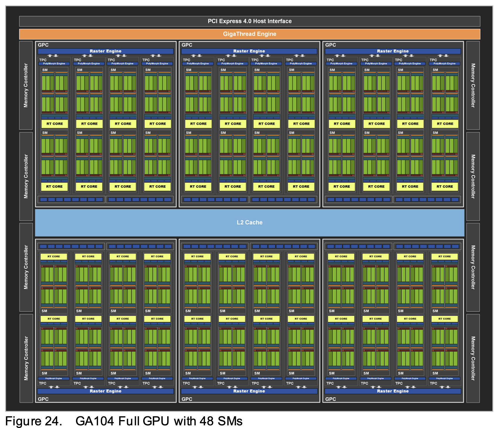
- GPCs: 6
- TPCs: 23
- SMs: 46
- CUDA Cores / SM: 128
- CUDA Cores / GPU: 5888
- Tensor Cores / SM: 4
- Tensor Cores / GPU: 184
- Peak FP16 Tensor TFLOPS with FP16 Accum: 81.3/162.6
- Peak INT8 Tensor TOPS: 162.6/325.2
- L1 Data Cache / Shared Memory: 5888
- L2 Cache Size: 4096 KB
- Register File Size: 11776
----------------------------------------------------
----------------------------------------------------
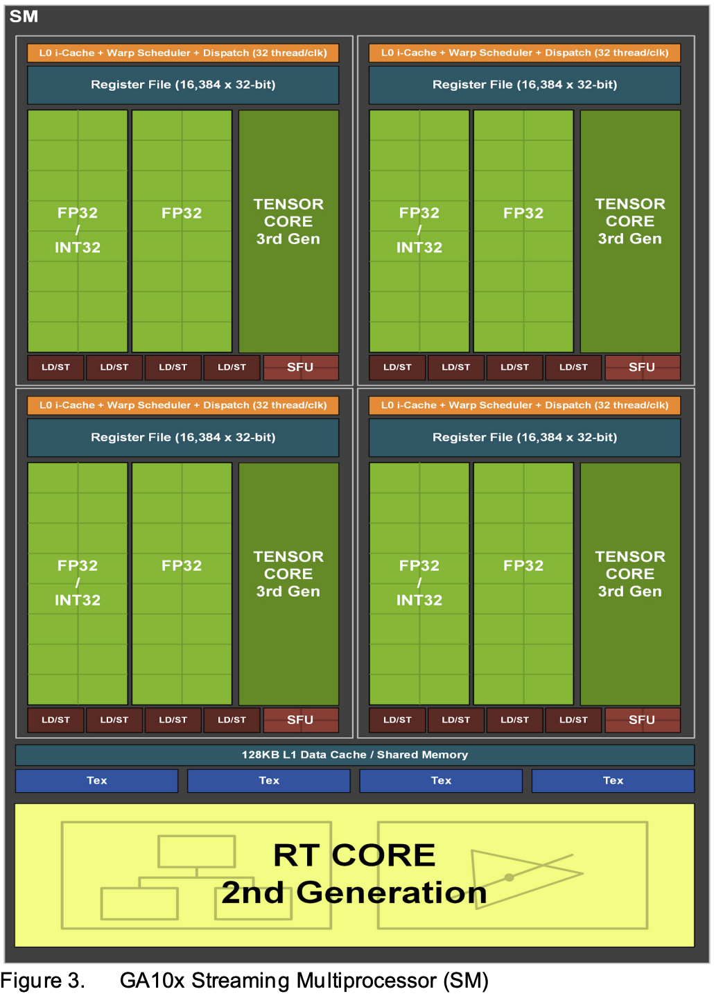
SMs
each SM in ga10x contains 128 CUDA Cores, 4 Tensor Cores, a 256 KB Register
file, 128 KB L1/shared mem
the ga10x SM is partitioned into 4 processing blocks or partitions, each with
a 64KB register file, an L0 instruction cache, one warm scheduler, one
dispatch unit, and sets of math and other units
the combined partitions make up the 128KB L1 data cache/shared mem subsystem
----------------------------------------------------
in last gen, each SM partition only had 1 datapath for FP32 ops
ampere has FP32 processing on both datapths, doubling the peak processing rate
for FP32 ops
one datapath in each partition consists of 16 FP32 CUDA Cores capable of
executing 16 FP32 operations per clock
the other datapath in each partition consists of both 16 FP32 cuda cores and
16 int32 cores, capable of executing either 16 fp32 or 16 int32 per clock
----------------------------------------------------
additional gpu arch notes
notes on SMs for Fermi architecture
things to learn:
- Streaming Multiprocessor (SM)
- warp and warp scheduler
- registers
notes
-
cuda core is the execute unit which has one float and one integer compute
processor
- the SM schedules threads in group of 32 threads called warps
- the warp schedulers means two warps can be issued at the same time
-
*registers are the fastest memory, L1 cache and shared memory is second
more notes:
-
a thread is the finest granularity, each thread has a unique
identifier within the block (threadIdx) which is used to select which data
to operation on. the thread can have a relatively large number of registers
and also has a private area of memory known as local memory which is used
for register file spilling and any large automatic variables
-
a block is a group of threads which execute together in a batch. this
level of granularity is that threads within a block can cooperate by
communicating using the fast shared memory. each block has a unique
identifier (blockIdx) which, in conjunction with the threadIdx, is used to
select data
-
a grid is a set blocks which together execute the GPU operation
-
a warp is a set of 32 threads. so if 128 threads per block, threads
0-31 will be in one warp, 32-63 in another warp, so on
-
threads within a warp are bound together, they fetch data together, so if
you can ensure that all threads fetch data within the same 'segment' then
you will only pay one memory transaction and if they all fetch from random
addresses you will pay 32 mem transactions
-
each block is launched on a SM, until it is done and the next block will be
launched. so if you have 30 SMs then the blocks will be scheduled across the
SMs dynamically
ensure when you launch a GPU function your grid is composed of large
number (at least hunders) to ensure it scales across the GPU
-
a SM can execute more than one block at any given time. this is why a SM can
handle 768(or more) threads while a block is only up to 512 threads
-
if the SM has the resources available then it will take on additional blocks
(up to 8)
----------------------------------------------------
directory